Researchers based in China have developed 120nm III-V high-electron-mobility transistors (HEMTs) with millimeter-wave broadband and satellite communication applications in mind [Huang Jie et al, J. Semicond., vol31, p074008, 2010]. The current-gain cut-off frequency (fT) was 141GHz and the maximum power gain cut-off was (fmax) 120GHz.
The research was carried out by scientists from Chinese Academy of Sciences Institute of Microelectronics and China s Southwest University in Chongqing. The researchers see their new indium gallium arsenide/indium aluminum arsenide (InGaAs/InAlAs) devices as being promising in millimeter-wave devices and integrated circuits .
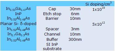 |
| Table 1: InGaAs/InAlAs HEMT epitaxial layer structure. |
The device structures (Table 1) were grown on semi-insulating indium phosphide (InP) substrates using molecular beam epitaxy (MBE). To make the transistors, the source and drain regions were formed first using the deposition and lift-off of six layers of alloyed metal (nickel, germanium, gold, germanium, nickel, gold). The resulting contact resistance was measured at 0.2 -mm using the transmission line model (TLM).
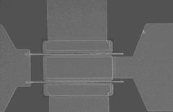 |
| Figure 1: Partial photograph of the InGaAs/InAlAs HEMT. |
To produce short gate lengths of ~100nm, the researchers developed a four-layer electron-beam resist process poly(methyl methacrylate) (PMMA), polymethylglutarimide (PMGI), ZEP520, polymethylglutarimide (PMGI). ZEP520 is a high-performance resist developed by Zeon Corp of Japan. The China researchers report that use of the bottom PMGI layer helps in the clean removal of the resist layers compared with a structure that has a ZEP520 bottom layer.
The gate (Figure 2) was recessed into the cap layer with a wet citric acid/hydrogen peroxide etch that was stopped by an InP etch-stop layer (selectivity InGaAs/InP ~160). The gate metal consisted of titanium, platinum and gold, which was deposited in an evaporation and lift-off process. A T-gate shape was used to reduce parasitic capacitance and resistance effects. The gate had a 120nm length and a 2x50 m width. Passivation was not used because the researchers wanted to avoid increasing the gate capacitance and thus impact the high-frequency performance.
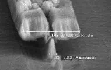 |
| Figure 2: SEM photo of T-shaped pattern of the InGaAs/InAlAs HEMT. |
The frequency performance was extracted from measurements made in the range 0.1 26.1GHz. The maximum power gain cut-off was determined from measurements made at a drain source voltage of 1.5V and a gate source voltage of 0.5V. Parasitic effects were de-embedded from the measurements. (Semiconductor Today)
Related News
Photos
More>>


trade
- Human Remains from China Indicate Modern Human Emerged Much Earlier Than
- CAS to Strengthen International Cooperation in 12th Five-year Plan Period
- NATURE: China Pushes for the Proteome
- In Ground-Based Astronomy s Final Frontier, China Aims for New Heights
- Ex-situ Conservation of Yangtze Finless Porpoises Goes well in Tian-e-zhou Baiji
market
finance
- Cosmic Magnifying Lenses Distorts the View of the Most Distant Galaxies
- Two Chinese Academicians Win Nation's Top Science Prize
- New Long-Tailed Pterosaurs Found in Western Liaoning, China
- Speeding up Electrons in Solar Cells
- IVPP Research Ranks among Discover Magazine's Top 100 Science Stories of 2010