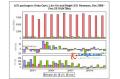
LED maker Epistar has demonstrated R&D results for a high-voltage HV LED chip that enables cold-white 5000K LEDs to reach 162 lm/W.
The chip is described as a monolithically-integrated, DC multiple-array chip LED for high-voltage applications. Epistar expects the product to reach the mainstream in general lighting applications.
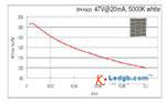
Epistar enables 162 lm/W white LED
The luminous efficacy of 162 lm/W was achieved for a drive current of 20 mA and voltage of 47V, corresponding to 0.94W power consumption. Under these conditions, the 45-mil 1.1x1.1 mm chip produced 152 lm see graph
Epistar says that the HV-LED has advantages of lower power consumption compared with traditional LEDs, as well as higher wall-plug efficiency, because of its robust new high-voltage chip design. The flexibility of voltage and current adjustment of HV-LED can simplify the LED package and circuit design, and its overall efficiency is therefore enhanced, the company says.
SMASH project reports progress
The SMASH project has published its second newsletter. SMASH aims to establish disruptive approaches to fabricating LEDs that exploit nano-structured materials to realize high-efficiency and low-cost devices. These will be achieved by epitaxial growth of LED structures on ultra-low-defect nano-structured templates and by the development of LEDs based on nano-rod emitters. These approaches will have large impact on manufacturing costs because they enable growth on large-area, low-cost substrates such as silicon.
One crucial step over the past 6 months has been the demonstration of position-controlled growth of n-face GaN nanorods by MOVPE. This work was performed by Osram Opto Semiconductors in close collaboration with the Technical University Braunschweig.
As well as the newsletter, the SMASH website contains a review of the International Workshop on Nitride Semiconductors 2010 September 19-24, 2010
Sumitomo Electric develops 6-inch GaN substrates
Sumitomo Electric Industries has developed the world's first 6-inch-diameter GaN gallium nitride substrates to be used for white LEDs. According to a Japan Corporate News Network article.
Previously, the company produced 2-inch GaN substrates for blue-violet lasers, which enabled production of the first Blu-ray DVD players. Sumitomo Electric began large-scale production of 2-inch GaN substrates for use in white LEDs, and has also been developing larger-diameter GaN substrates.
The front face of the newly developed 6in GaN substrates is a polarized c-plane. Sumitomo Electric has ongoing development efforts to bring this material into large scale production and expects that these materials will find widespread use for both white LEDs and power devices.
Nanorod arrays enable natural-white LEDs
Researchers at National Tsing-Hua University Hsinchu, Taiwan have developed a new recipe for a phosphor-free white LEDs, according to an article on OptoIQ. The devices use GaN nanorod arrays on silicon Si substrates as a template for growing strain-free InGaN/GaN nanorod heterostructures that eliminate piezoelectric polarization effects.
Nanorod arrays enable natural-white LEDs
Verticle launches first hexagonal LED chip
Verticle Inc of Dublin, CA, USA, has announced what it claims is the first hexagonal-shaped LED chip, according to an article on the Semiconductor Today magazine. The Honeycomb LED Chip is a vertically-structured InGaN-based blue LED chip developed especially for high-power applications. CEO Mike M.C. Yoo believes that, compared with conventional square- or rectangular-type LEDs, a hexagonal LED chip yields multiple benefits regarding cost, light output efficiency, and beam profile.
LED packaging and assembly
ElectroIQ has an interview with Jan Vardaman, president of TechSearch International. Speaking at the MEPTEC Semiconductor Packaging Roadmaps conference Santa Clara, CA on Nov 10 Vardaman said that there is room for improvement in LED packaging and assembly.
In this podcast interview with Debra Vogler, senior technical editor, Vardaman discusses sapphire and SiC substrates, as well as the various singulation methods currently in use by LED manufacturers. Other subjects for discussion include the size of substrate wafers, and standards for LED manufacturing.
Blue semipolar GaN LEDs
Researchers at the University of California, Santa Barbara UCSB and Mitsubishi Chemical Corporation Ibaraki, Japan have developed a backside-roughening technique for blue semipolar gallium-nitride GaN -based LEDs. This makes the devices comparable to commercial wurtzite c-plane LEDs in terms of both performance and manufacturing methods, according to an article on the OptoIQ website.
Related News
Photos
More>>

trade
market
- Osram Opto expands LED capacity with 6-inch conversion
- LED phosphor suppliers are affected by China's rare-earth export quotas
- YoungTek posts sequential growth in February revenues, Single Well revenues
- Digital Lumens supplies LED lighting systems for 7 Americold warehouses
- Guangdong to Relax Family Policy by 2030